The solar silicon wafer acts as the main base for most photovoltaic (PV) cells. It turns sunlight into power through special semiconductor steps. Makers create it from very clean crystalline silicon. They cut this into thin wafers. In the current world of clean energy, these wafers support the solar field. They affect how well it works, how much it costs, and how easily it grows. The market for solar silicon wafers has expanded quickly. This happens because of worldwide goals to cut carbon and better ways to slice wafers and design cells. But even with this growth, people now wonder if the market size numbers really show true demand. Or do policies and too much supply push them up?
Overview of the Solar Silicon Wafer Market Landscape
The solar silicon wafer market forms a tricky network. It links early polysilicon makers with later cell and module builders. Experts divide it by crystal kind, wafer size, and areas where production happens.
Current Market Structure and Segmentation
The market splits mostly into monocrystalline and polycrystalline wafers. Monocrystalline wafers lead because they work better. They have fewer flaws, so they fit high-power modules for big projects. Polycrystalline wafers still matter for cheap uses. But they lose ground as monocrystalline prices drop to match.
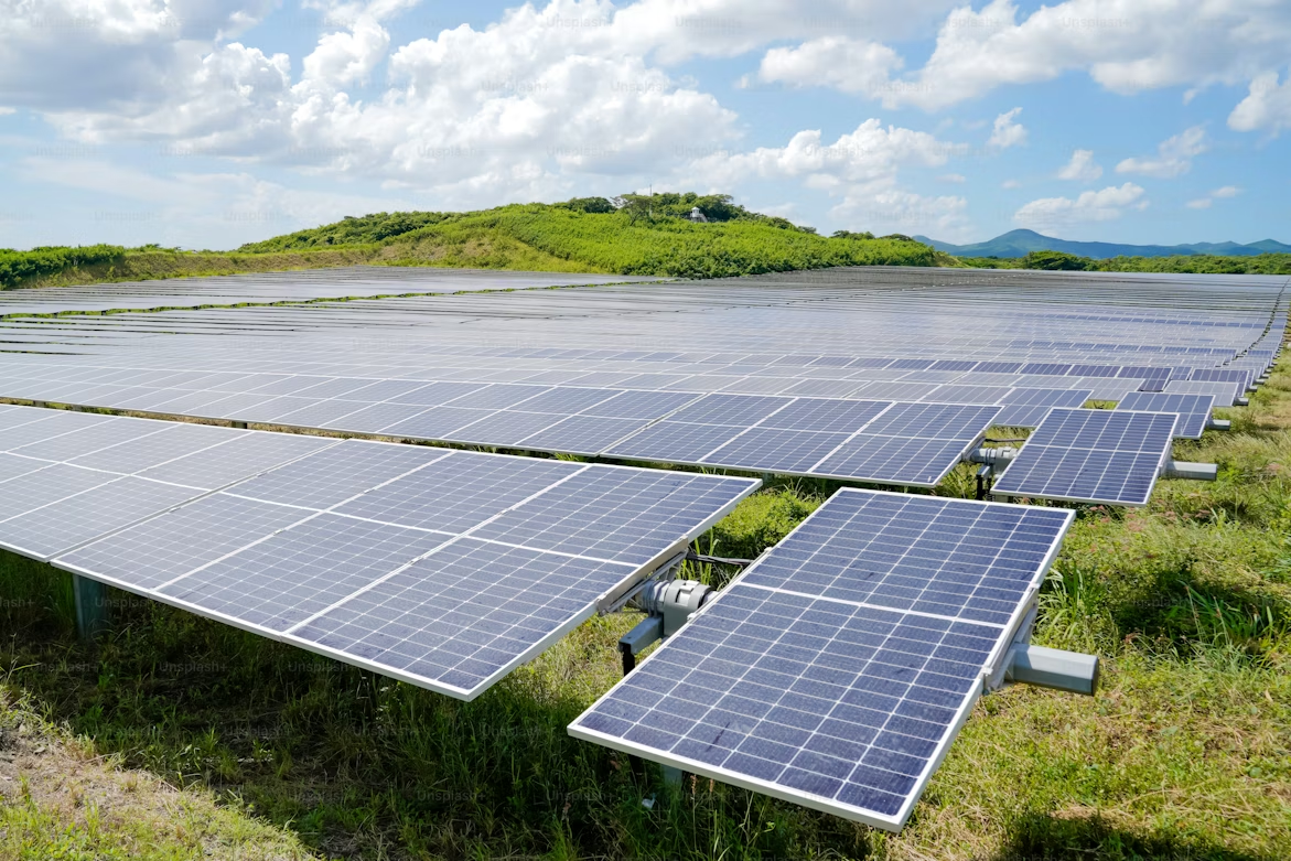
Wafer sizes have changed from the old M2 (156 mm) to bigger ones like M10 (182 mm) and G12 (210 mm). Bigger wafers give more power per module. They do this by adding surface space without raising costs too much. These shifts make cell and module lines need new tools to fit the sizes.
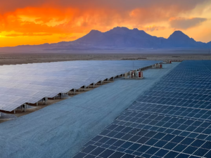
In different areas, Asia-Pacific runs both making and using. China makes over 90% of all wafers worldwide. Taiwan and South Korea come next. They supply special high-quality or unique wafer types.
Key Industry Drivers and Restraints
Growing use of solar stays as the top push for growth. Countries chase zero-carbon aims. The cost of solar power keeps falling. This draws money into PV setups. But prices of raw stuff can change fast. Polysilicon is a big example. It hurts profits for wafer makers since silicon takes a lot of the total cost.
New ideas in tech also set who wins. Better ways to pull crystals, cut with diamond wires, and add protective layers boost output. They cut waste too. However, these steps need big money for changes. Small companies often can’t pay for them.
Assessing Whether Market Size Reflects True Global Demand?
Reports show the market size keeps growing. Yet these numbers might not fully match real use patterns in areas or tech types.
Discrepancies Between Production Capacity and Actual Consumption
Too much capacity is a common problem in the solar silicon wafer area. Big Chinese makers grew fast from 2021 to 2023. They expected huge demand that didn’t come as quick. So stocks built up. Prices fell hard.
In many spots, making focuses on selling abroad. It doesn’t match home setup rates. For example, China makes way more wafers than it uses inside each year. It sends extras to places like Southeast Asia or Europe. There, local making is small.
Government help can twist demand signs more. It boosts setups for a short time. Or it pushes making beyond what lasts.
Evaluating Demand Indicators Beyond Market Size Metrics
Added PV capacity shows real demand better. It counts systems put on grids or roofs. This measures true use, not just sent parts. Watching module sends with wafer buys spots gaps between early supply and later take-up.
Long deals for power sales also steady demand. They lock in future sales from solar jobs. This keeps use going even when quick helps end.
Technological Advancements Shaping Market Dynamics
Changes in tech have always changed who leads in the solar chain. The move to monocrystalline shows how better work drives big shifts in making setups.
Transition from Polycrystalline to Monocrystalline Wafers
Monocrystalline wafers give higher change rates to power. They often go over 22% at the cell stage. This comes from their even atom setup. It cuts losses from electron jumps. As costs drop from big-scale making and better block casting, price gaps with poly ones almost vanish.
This change forces makers to update old lines. They add new crystal growth ovens. Or they use designs that fit PERC (Passivated Emitter Rear Cell). All to stay in the game.
Emerging Wafer Technologies and Their Market Impact
Larger Wafer Formats (M10, G12) Adoption Trends
Bigger sizes like M10 (182 mm) and G12 (210 mm) turn common now. They cut cost per watt. How? By giving more power per cell group. But going bigger brings fit issues with old module build lines. Those lines fit small wafers.
Thin Wafer Innovations and Yield Optimization
Work on thin wafers aims to use less silicon. It keeps strength and power the same. New diamond wire cuts lower kerf loss. That’s the waste between slices. So yields per block rise. Thinner wafers also weigh less to ship. But they break easier when handled. So better pack ways are needed.
Regional Insights into Supply–Demand Equilibrium
Uneven spots in areas shape price moves and trade paths in the global solar chain.
Asia-Pacific as the Core Manufacturing Hub
Asia-Pacific rules making because of tight factory groups in China’s places like Jiangsu and Yunnan. Cheap power there helps the power-hungry block pulling. Taiwan adds clean wafer tech. South Korea puts money into top-grade items for special junction cells.
Local rules with tax cuts or easy loans keep pushing early investments. This happens even with worries about extra supply now and then.
North America and Europe’s Evolving Demand Patterns
North America’s need jumps from state rules on clean power mixes. Federal tax breaks help big setups too. Europe’s Green Deal rules push new adds the same way. But it brings in most wafers from outside. Local making ability is low.
New plans try to bring some chain parts home. They use team-ups or government-backed plants. Yet these stay small next to Asian amounts.
Emerging Markets’ Role in Future Demand Expansion
India’s big solar plans in its National Solar Mission make it a key for growth in wafer use. But home making lags behind setup needs. In Southeast Asia, spots like Vietnam grow later build spots. Latin America sees more take-up. Groups from other countries fund clean energy shifts.
Economic and Policy Factors Influencing True Market Reflection
Money factors mix with rule setups. They shape how well market size shows real end-user needs.
Trade Policies, Tariffs, and Supply Chain Realignments
Trade limits between big countries change flows of wafers and cells worldwide. Taxes on items from China make some companies build plants abroad in spots like Malaysia or Cambodia. This shifts where fights happen. But it doesn’t change total use amounts.
Efforts to make things local get help from country plans. They aim to keep supply safe from world fights. But they might break the good ways from years of world trade.
Government Incentives and Carbon Neutrality Goals
Helps from governments stay key to spark seeming demand. They use set prices for power or tax breaks linked to clean setup steps. But these can push up short stats. Setups rush before helps end. This doesn’t show true money worth.
Promises for no carbon by 2050 in big countries still back long growth. They support steady need even after quick fixes.
Strategic Outlook for Industry Stakeholders
Matching plans with true signs matters as ups and downs stay in chains and rules.
Aligning Production Strategies with Authentic Demand Signals
Makers need good guess tools. These should mix live setup info. Don’t just use hoped sends. Clear talks between polysilicon sellers, wafer builders, cell makers, and job leaders can cut boom risks. Those risks hurt money for all.
Keeping growth ideas with real use views stops wrong use of stuff. This avoids waste in guess rushes from help loops. Not from true power grid needs.
Long-Term Growth Opportunities in Next-Generation Photovoltaics
Integration with Tandem Solar Cells (Perovskite–Silicon)
Mixed perovskite–silicon tandem tech might change wafer rules later. They need tuned surface shapes. These fit multi-layer builds that hit over 30% power rates. Single-layer ones can’t reach that now.
Circular Economy Approaches in Silicon Recycling
Plans to reuse from old panels get back key silicon stuff. This cuts need for new raw items. It steadies input prices when goods swing. It’s a big step for green growth in world PV use. No big strain on raw needs.
FAQ
Q1: What distinguishes monocrystalline from polycrystalline solar silicon wafers?
A: Monocrystalline wafers are made from single-crystal structures offering higher efficiency; polycrystalline ones contain multiple crystals making them cheaper but less efficient.
Q2: Why do larger wafer sizes matter?
A: They produce more power per module area which lowers cost per watt though they require equipment upgrades along the value chain.
Q3: How does government policy affect true market size?
A: Subsidies can inflate short-term figures by encouraging installations ahead of deadlines without guaranteeing sustained demand afterward.
Q4: What regions dominate global production?
A: China leads overwhelmingly followed by Taiwan and South Korea forming Asia-Pacific’s manufacturing backbone for solar silicon wafers.
Q5: How might recycling influence future markets?
A: Efficient silicon recovery processes will reduce raw material dependence stabilizing prices while supporting circular economy goals within renewable energy sectors.